Loading overlay
Menu button back to Home page
Header image Energie-to-Components
The Carlo Gavazzi Group

Diffusion furnaces

Diffusion furnaces play a vital role in semiconductor manufacturing, utilizing precise heating processes involving radiant and convection heating. The temperature in the different zones must be tightly controlled as well as temperature gradients to ensure uniform diffusion of impurities into silicon wafers. These furnaces also carefully manage temperature ramp-up and cool-down rates to prevent thermal stress on the wafers. Modern diffusion furnaces now include advanced controls to monitor critical process parameters on real-time thereby avoiding process defects at this critical stage of the semiconductor manufacturing process.

Vapor deposition equipment (ALD, CVD, PECVD)

Another critical process in the silicon wafer production is known as vapor deposition. This process involves thermal processes that heat the source materials (known as precursors) to a vapor state and then allowing them to condense on the wafer substrate.  This method enables precise and controlled thin-film coatings for both silicon wafers as well as optical coatings such as displays and PV arrays. Vapor deposition systems involve various stages each requiring precise temperature control to ensure uniform and high quality depositions. 

Silicon wafer sorting machines

Silicon wafers are very fragile and precise detection is required to detect the position and presence of the wafers during wafer transfer and also during automatic loading and unloading operations. In most cases, the installation space is very limited and any detection sensors need to have flexible mounting and must be easily tuned.  Another critical feature is that of high immunity to external interference as the latter might result in mis-detection and high scrap costs. 

Silicon wafer cleaning equipment

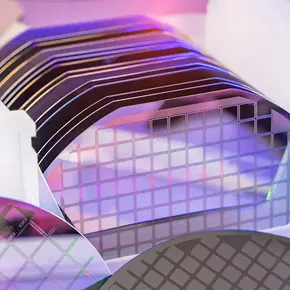
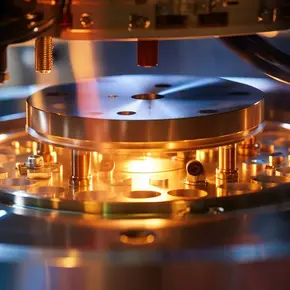
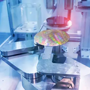
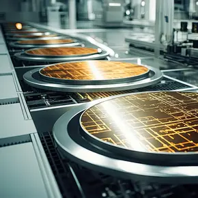
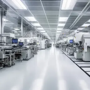
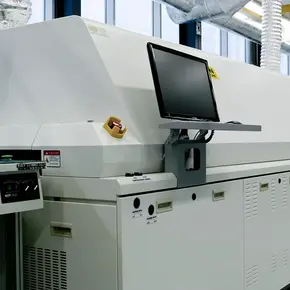
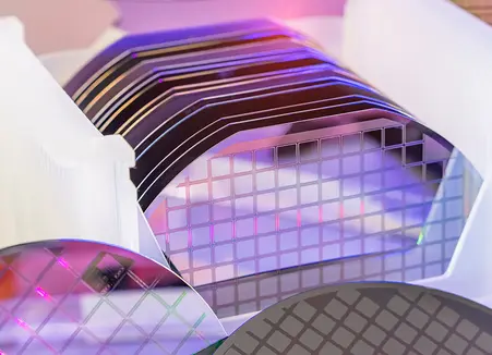
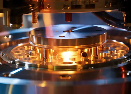
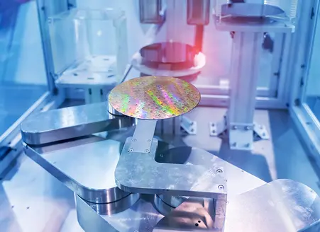
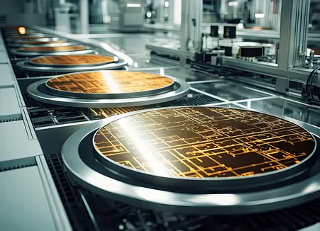
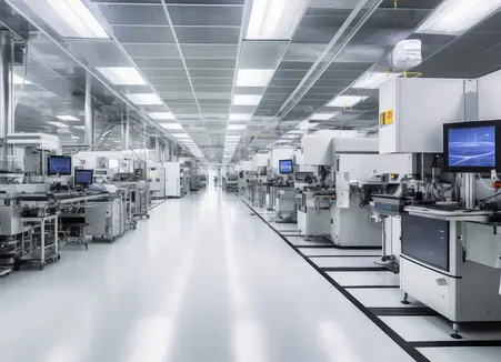
Silicon wafer cleaning equipment is essential in the semiconductor industry to maintain the purity and integrity of wafers. These machines utilize a combination of chemical, mechanical, and ultrapure water-based processes to remove contaminants, particles, and organic residues from the wafer surface. The equipment typically includes ultrasonic baths, chemical tanks, spin rinse dryers, and scrubbers, all designed to achieve a high level of cleanliness. Precision is paramount, as even the tiniest impurities can affect semiconductor performance. Clean wafers result in improved yields and quality, making these cleaning systems indispensable in semiconductor manufacturing.

Test equipment

Semiconductor test equipment plays a critical role in assessing the functionality and performance of integrated circuits and semiconductor devices. Heating components are often integrated into test systems for various purposes. One primary function is temperature testing, which subjects the semiconductor device to different temperature ranges to evaluate its performance under various operating conditions.
Heating elements, such as resistive heaters or Peltier devices, are used to precisely control the temperature of the device under test. This is crucial because many semiconductor devices exhibit different behaviors at different temperatures, and thorough testing at extreme temperature ranges is necessary to ensure reliability.

Solder reflow ovens and wave soldering machines

Reflow ovens are commonly used for surface-mount technology (SMT) components. These ovens use a conveyor system to pass PCBs through a carefully controlled thermal profile. The oven's precise temperature zones melt the solder paste, creating strong electrical connections between components and PCBs. This process ensures reliability and consistency, making it suitable for high-density and miniaturized electronics. Wave soldering, on the other hand, is primarily used for through-hole components. It involves a molten solder wave that PCBs are passed over. 

Climatic chambers

Climatic chambers are widely used in semiconductor testing and reliability assessment. These chambers provide controlled environments where semiconductor devices are subjected to different levels of temperature  and humidity to expose any design flaws or lifetime issues. Climatic chambers can also be used as part of a burn-in system where the devices under test (DUT) will also be subjected to both temperature and electrical stress to simulate a real-world application.  By accelerating certain physics of failure, manufacturers can ensure that the final product will meet customer specifications under different use conditions.